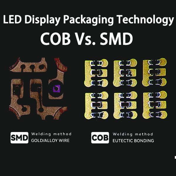
In LED display packaging technology, COB (Chip on Board) and SMD (Surface Mounted Devices) are the two main technical methods.
Here is a detailed introduction and comparison of the two technologies:
COB packaging technology
COB packaging technology is a technology that directly packages LED chips on PCB (Printed Circuit Board). The characteristic of this technology is that the LED chip does not exist in the form of traditional lamp beads, but is directly implanted into the PCB board. Specifically, COB packaging is to hand-mount semiconductor chips and integrate them on MCPCB (metal-based printed circuit board). The electrical connection between the chip and the substrate is achieved by wire stitching and covered with resin to ensure reliability.

The advantages of COB packaging technology are mainly reflected in the following aspects:
Improve luminous light color
Since the LED chip is directly integrated into the PCB board, the distribution and color of the light can be better controlled, thereby improving the light color of the LED display.
Reduce risk
Due to the tight integration of the chip and the PCB board, COB packaging technology can reduce the risk of damage caused by vibration, impact and other factors.
Cut costs
Compared with discrete LED devices, COB light source modules can save LED primary packaging costs, light engine module production costs and secondary light distribution costs in applications. Actual estimates can reduce light source costs by about 30%.
Ultra thin
According to the actual needs of customers, PCB boards with thicknesses ranging from 0.4-1.2mm can be used to reduce the weight to at least 1/3 of the original traditional products, which can significantly reduce structural, transportation and engineering costs for customers.
Anti-collision and compression resistance
COB products directly encapsulate the LED chip in the concave position of the PCB board, and then encapsulate and solidify it with epoxy resin glue. The surface of the light spot is raised into a spherical surface, which is smooth and hard, and is impact-resistant and wear-resistant.
Wide viewing angle and strong heat dissipation capability
It uses a shallow well spherical surface to emit light, and the viewing angle is greater than 175 degrees, close to 180 degrees; at the same time, the lamp is packaged on a PCB board, and the heat of the wick is quickly transferred through the copper foil on the PCB board, which has excellent heat dissipation performance.
SMD packaging technology
SMD packaging technology, that is, surface mount device technology, is a packaging technology that encapsulates SMT lamps encapsulated in LED chips at a certain distance in the same colloid to form a display module. At present, indoor full-color LED screens mainly use surface-mounted three-in-one SMD.
Features of SMD packaging technology include:
High maturity
SMD packaging technology has been launched for a long time and has high technological maturity, so the cost is relatively low.
Various dot spacing options
The dot pitch of the SMD-packaged LED display can be as large as P20, or as small as P1.25, with various options.
However, SMD packaging technology also has some shortcomings, such as low product reliability, poor surface protection, and high defective pixel rate.
Comparison of COB and SMD

Packaging methods are different
COB packaging directly encapsulates the LED chip on the PCB board, while SMD packaging encapsulates the SMT lamp encapsulated in the LED chip in the same colloid.
Point spacing is different
SMD packaging has various dot pitch options, but COB packaging is mainly aimed at small pitch products of P1.25 and below.
Costs vary
Although SMD packaging costs are relatively low, COB packaging may be more cost-effective in some application scenarios due to its advantages in saving packaging costs.
In summary, COB and SMD packaging technologies each have their own characteristics and advantages, and the specific choice should be determined based on actual application scenarios and needs.


